
In this guide
AI has a physical stack
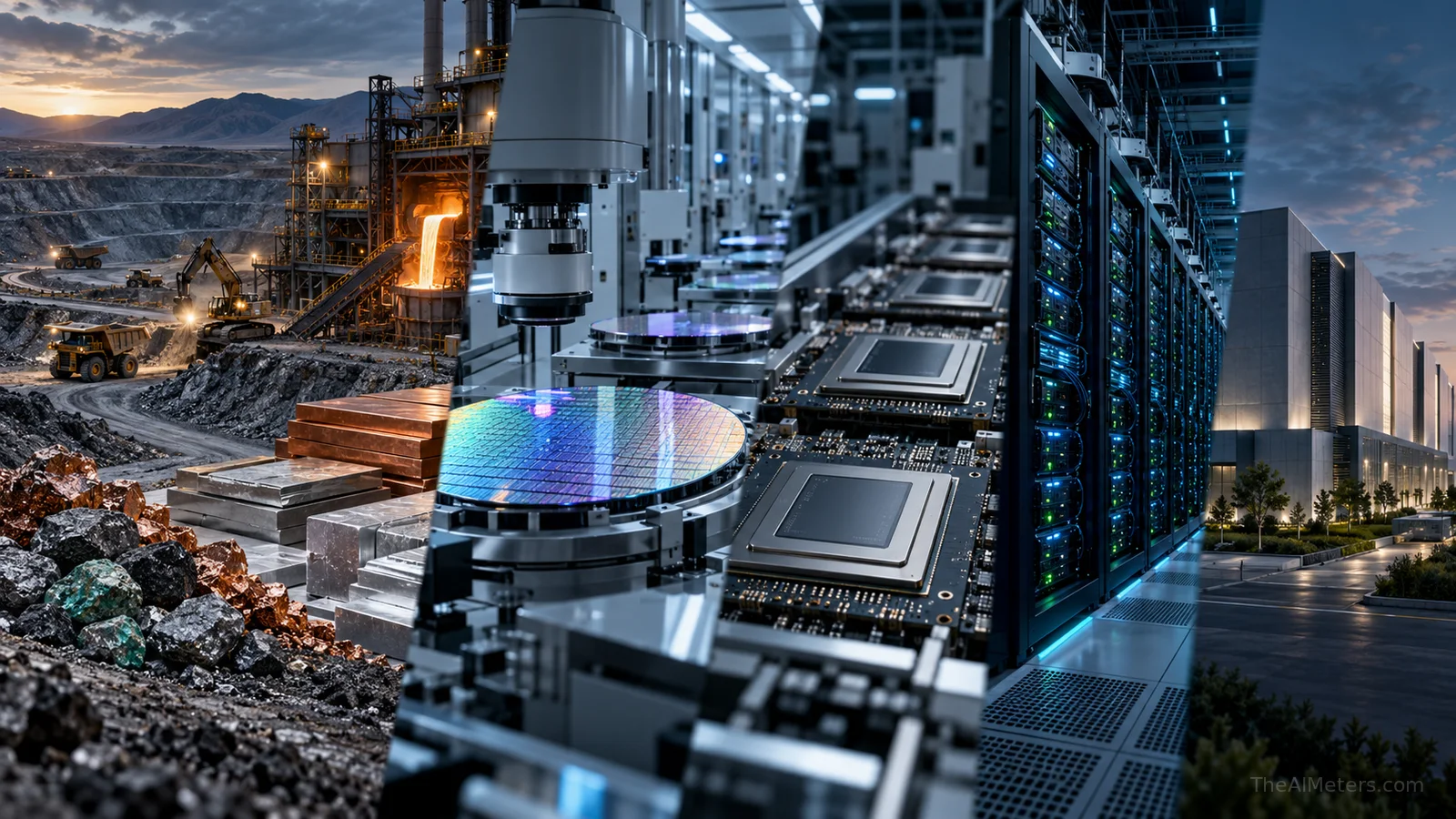
An AI model may appear as software on a screen, but running it requires a long physical chain. Mines and refineries supply raw materials; semiconductor plants fabricate processors and memory; equipment manufacturers assemble servers; and datacenters provide power, networking and cooling.
This distinction matters because operational electricity is only one part of the lifecycle. Before a server processes its first prompt, energy and materials have already been used to manufacture its chips, circuit boards, power supplies, storage, cooling hardware and the building that contains them.
No single number captures this entire footprint. Boundaries vary between studies: some count only computing equipment, while others include buildings, electricity infrastructure, water, networks, replacement cycles or end-of-life treatment. A credible estimate must state what is included.
Advanced chips carry an upstream footprint
AI accelerators combine processors, high-bandwidth memory, circuit boards, cooling components and complex packaging. Producing them requires extremely controlled manufacturing, repeated processing steps, ultrapure water, electricity, specialty gases and chemicals.
Smaller semiconductor process nodes can deliver more computing performance, but fabrication does not become impact-free. The Shift Project's review notes that energy, water and greenhouse-gas impacts per unit of silicon area can rise as manufacturing processes become more advanced, while public product data remain incomplete.
Efficiency must therefore be considered at two levels. A newer accelerator may perform the same workload with less electricity, yet replacing equipment early also creates a new manufacturing footprint. The best outcome depends on workload efficiency, useful lifetime, utilization and what happens to the displaced hardware.
AI hardware uses many metals and concentrated supply chains
Servers contain steel, aluminum, copper, silicon and many smaller quantities of specialized materials used in electronics, batteries, magnets, connectors and power systems. The ADEME research summarized by The Shift Project notes that more than 50 metals can be present across digital equipment.
The issue is not simply the mass of each material. Mining, refining and component production occur in different countries and can carry very different energy, water, pollution, labor and governance conditions. A small quantity of a difficult-to-refine material can have an impact that is not visible from the final server's weight.
Supply chains are also geographically concentrated. Stanford's AI Index highlights the concentration of advanced semiconductor fabrication and AI computing capacity in a small number of countries. That concentration can create industrial bottlenecks and distribute benefits and environmental burdens unevenly.
The building around the servers also counts
AI infrastructure requires more than racks of accelerators. Datacenters use concrete, structural steel, electrical substations, backup systems, batteries, transformers, switchgear, cables, pumps, heat exchangers, cooling towers and network equipment.
Embodied emissions from manufacturing and construction are often smaller than operational emissions on a fossil-intensive grid, but they are not negligible. Their relative importance grows when electricity becomes lower-carbon, because concrete, steel, electronics and replacement equipment remain part of the lifecycle.
Facility and IT equipment also age at different rates. A 2026 filing for Google's Agate datacenter in Nebraska describes a typical facility design life of more than 25 years and a 30-to-50-year structural shell, while internal computing, electrical and cooling subsystems are replaced or modernized in modules. This is an operator description of one datacenter, not a universal industry rule.
Hardware replacement creates a second footprint
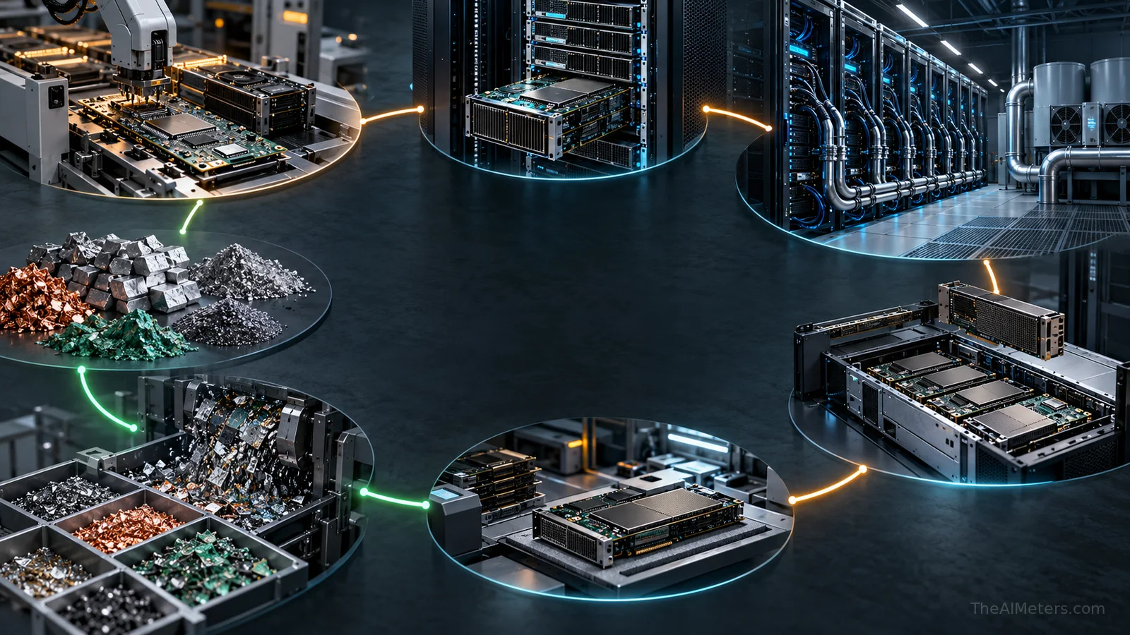
Demand for faster accelerators can shorten practical replacement cycles even when older hardware still operates. New equipment may improve performance per watt, but manufacturing it requires another round of materials, industrial energy, transport and installation.
Retired hardware does not automatically become waste. Some servers and components can be reassigned to less demanding workloads, refurbished, resold or used for spare parts. Secure data handling, compatibility, energy efficiency and maintenance costs determine whether reuse is practical.
What cannot be reused enters the electronic-waste system. The UNU-INWEH report cites a projection of up to 2.5 million tonnes of AI-related electronic waste per year by 2030. This is a forward-looking estimate rather than a measured current total, and it depends heavily on deployment and replacement assumptions.
Can AI's material footprint be reduced?
The most direct levers are longer useful hardware lifetimes, high server utilization, repairable and modular systems, reuse before recycling, cleaner manufacturing and better recovery of valuable materials. Operators can also publish product-level footprints and replacement policies so improvements can be verified.
Software decisions matter too. Smaller fit-for-purpose models, efficient inference, batching, quantization and routing simple tasks to lighter systems can deliver useful work from existing hardware. Efficiency only reduces the total footprint when growth in demand does not erase the savings.
Better measurement is essential. Reporting should separate operational electricity from embodied emissions, identify lifecycle boundaries and distinguish company-wide averages from facility-level data. The goal is not to attach one exact material number to every prompt, but to make infrastructure decisions more transparent and comparable.
Further reading and references
- United Nations University — Environmental Cost of AI's Energy Use
- The Shift Project — AI, data and computing infrastructure
- Stanford AI Index 2026
- International Energy Agency — Energy and AI
- US EPA — Electrical and electronic components manufacturing
- Nebraska Data Center 2026 Annual Report — Agate LLC